


")


Modern electronics continue to grow in complexity, with higher component densities, finer pitch components and increasingly demanding performance requirements. As a result, PCB design has become a critical factor in ensuring manufacturability, solder joint reliability and long-term product performance.
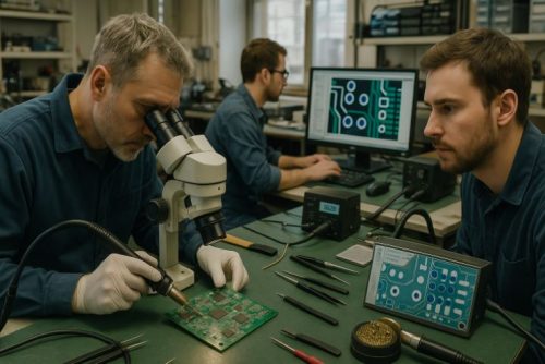
For individuals working within the soldering sector, including those involved in assembly, inspection and rework, a strong understanding of PCB design principles improves decision-making throughout the production cycle.
By studying structured PCB design courses at an established electronics training centre, technicians gain valuable insight into how layout choices, pad geometry, trace routing and thermal behaviour affect soldering outcomes.
Therefore, in this blog, we will examine the evolving landscape of PCB design, the key competencies developed through formal training, the influence of design on soldering quality, the role of CAD tools and industry standards, and the growing importance of design education for professionals in high-reliability electronics manufacturing.
The Importance of PCB Design Courses in Modern Electronics
 The Evolving Landscape of PCB Design in Modern Electronics
The landscape of PCB design has transformed significantly in recent years as manufacturers adopt finer pitch components, multi-layer architectures and increasingly compact assemblies.
These changes are driven by demands for higher functionality, reduced form factors and improved thermal performance, all of which place new pressures on designers to create layouts that remain compatible with high-quality soldering processes.
As component density increases, the interaction between pad design, solder mask alignment, copper distribution and thermal pathways becomes far more sensitive to variation, which means that even small design inaccuracies can lead to assembly defects, cold joints or reflow inconsistencies.
For technicians and engineers working closely with soldering processes, particularly those involved in surface mount rework, understanding these design-driven challenges is essential.
PCB design choices directly influence how reliably solder paste is deposited, how components self-align during reflow and how easily assemblies can be inspected or repaired.
As modern electronics continue to trend toward miniaturisation and higher reliability standards, the relationship between PCB design and practical soldering outcomes grows stronger, making comprehensive design education increasingly valuable across the production and rework environment.
Core Competencies Developed Through Professional PCB Design Courses
Professional PCB design courses equip learners with a comprehensive understanding of how electrical, mechanical and thermal factors converge within a printed circuit board.
Students develop the ability to evaluate component footprints, optimise pad geometries and route traces with precision to support stable signal integrity and high-quality soldering outcomes.
These courses also strengthen understanding of copper balancing, thermal dissipation strategies, via selection and the influence of layout decisions on manufacturability.
Such competencies form the foundation of effective board design and are crucial for preventing common assembly issues such as insufficient solder volume, misalignment or thermal shadowing during reflow.
In addition to theoretical knowledge, structured training provides hands-on experience using industry-standard CAD tools and design workflows. Technicians learn to interpret datasheets, apply design-for-manufacture principles and implement layer stack-up strategies that align with modern production capabilities.
By mastering these skills, individuals gain the ability to design boards that are both functionally robust and compatible with high-reliability soldering processes, which is essential in sectors that require precision, repeatability and strict adherence to quality expectations.
How PCB Design Influences Soldering Quality and Rework Complexity?
 PCB design has a direct influence on soldering quality because the geometry of pads, the alignment of solder mask openings, the balance of copper areas and the spacing between components determine how effectively solder paste can be deposited and how predictably it will behave during reflow.
Incorrect pad sizes can lead to issues such as insufficient solder, bridging or tombstoning, and inconsistent thermal distribution may affect wetting and joint strength.
When footprints are designed accurately and thermal behaviour is well controlled, solder joints form more consistently and with far greater reliability across a range of assembly conditions.
These same design factors also shape the complexity of rework once an assembly is complete. Dense layouts may reduce tool access for hot-air systems or micro-soldering equipment, and large areas of copper can absorb heat, making component removal slower and more difficult.
Thoughtfully designed boards provide adequate spacing, predictable thermal characteristics and accessible component positions, which enable technicians to perform effective rework with reduced risk of collateral heating or damage to surrounding areas.
The Integration of CAD Tools and Industry Standards in PCB Design Training
Modern PCB design training places strong emphasis on the use of specialist CAD platforms because these tools enable designers to create accurate and manufacturable layouts.
Through structured instruction, learners develop competence in schematic capture, footprint creation and rule-based routing, which allows them to define constraints for clearances, trace widths and controlled-impedance pathways.
These capabilities support stable electrical performance and help ensure that soldering processes operate within predictable and repeatable conditions during assembly.
Alongside software proficiency, effective training incorporates key industry standards that underpin reliable electronics manufacturing. Frameworks such as IPC-2221 for generic board design and IPC-7351 for component land patterns guide learners in producing layouts that improve solder joint integrity, inspection accuracy and overall manufacturability.
By combining CAD skills with established standards, PCB design courses equip technicians with the knowledge needed to create boards that align with modern production requirements and high-quality soldering expectations.
Conclusion
PCB design courses provide essential knowledge for professionals working across the soldering sector because they strengthen the link between layout decisions, assembly efficiency and long-term product reliability.
By developing competence in CAD tools, industry standards and design-for-manufacture principles, learners gain a deeper understanding of how electrical, mechanical and thermal considerations influence solder joint formation and rework complexity.
As modern electronics continue to advance in density and performance requirements, well-informed design practices remain fundamental to achieving consistent, high-quality outcomes in both production and repair environments, making structured PCB design training a valuable foundation for anyone involved in high-reliability electronics.


